A sensor is born
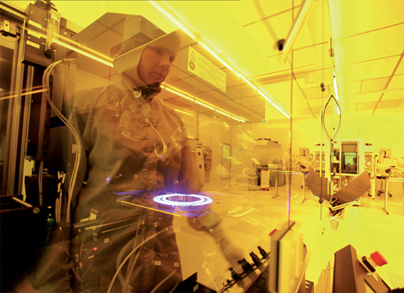
Advanced sensors are produced in SINTEF’s MiNalab. This image shows the process of photolithography, which is utilized to produce the sensors. A few seconds of powerful light enables the processing engineer to reproduce a delicate metal routing pattern from a mask to silicon wafers, which are covered with a light sensitive film. The patterns on the screen are on a micrometer scale. As ordi?nary white light destroys the film, the process must be performed in yellow light.
Source: Maaike M. Visser Taklo, SINTEF ICT