Building miniature lasers with nanowires
Impossibly small, accurate lasers could pave the way for new medical applications and electronics.
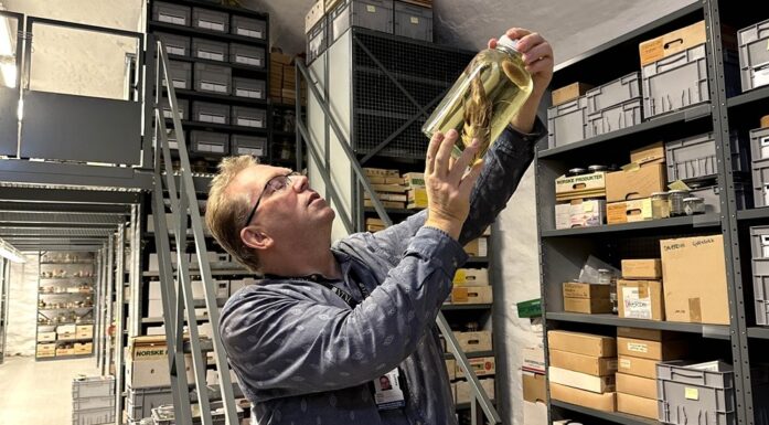
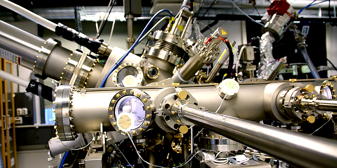
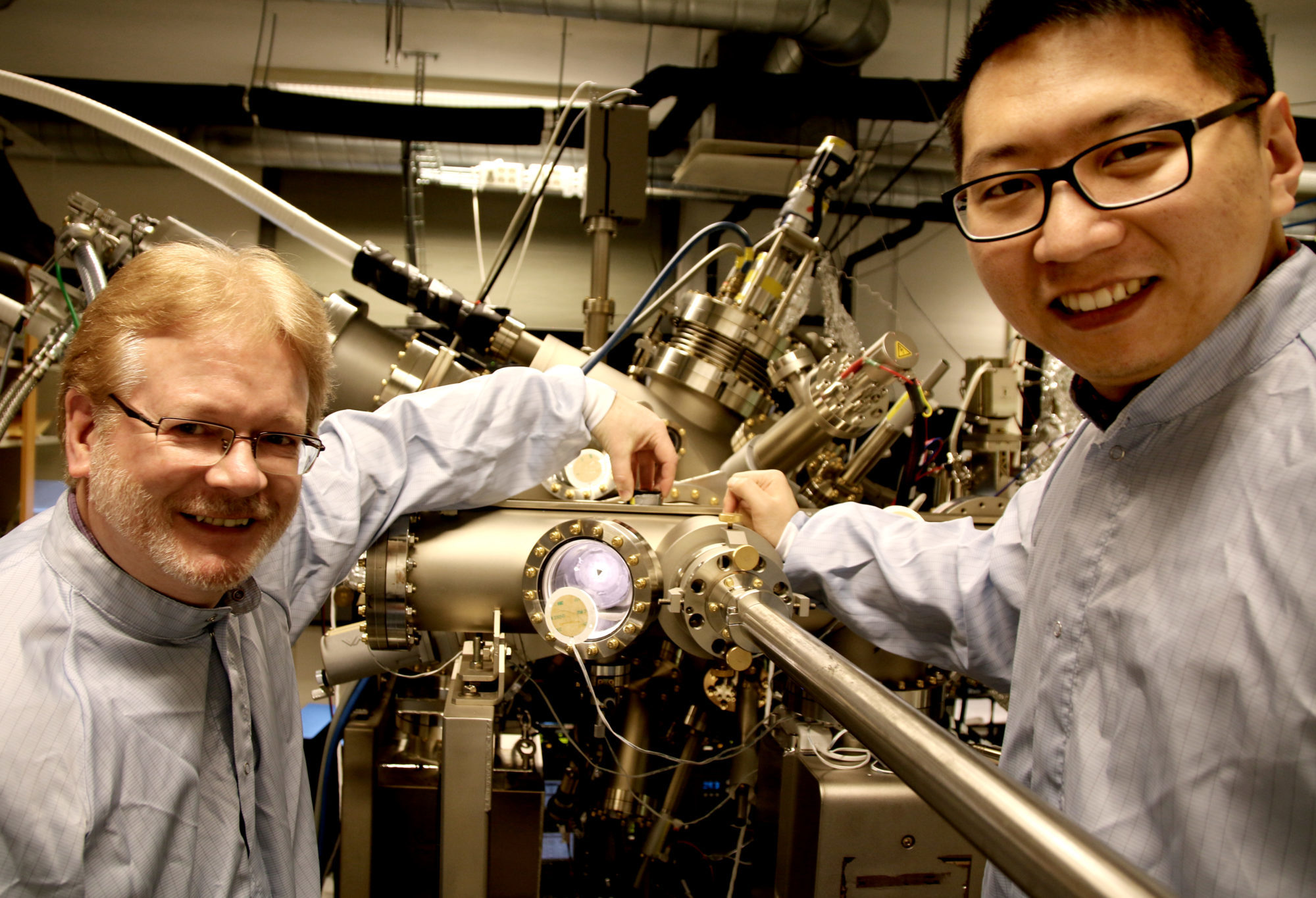
A large machine with all manner of assorted protruding pipes stands ready for action in one of the labs at NTNU’s Department of Electronic Systems. Some of the pipes are protected by insulating material, while others are wrapped in silver paper.
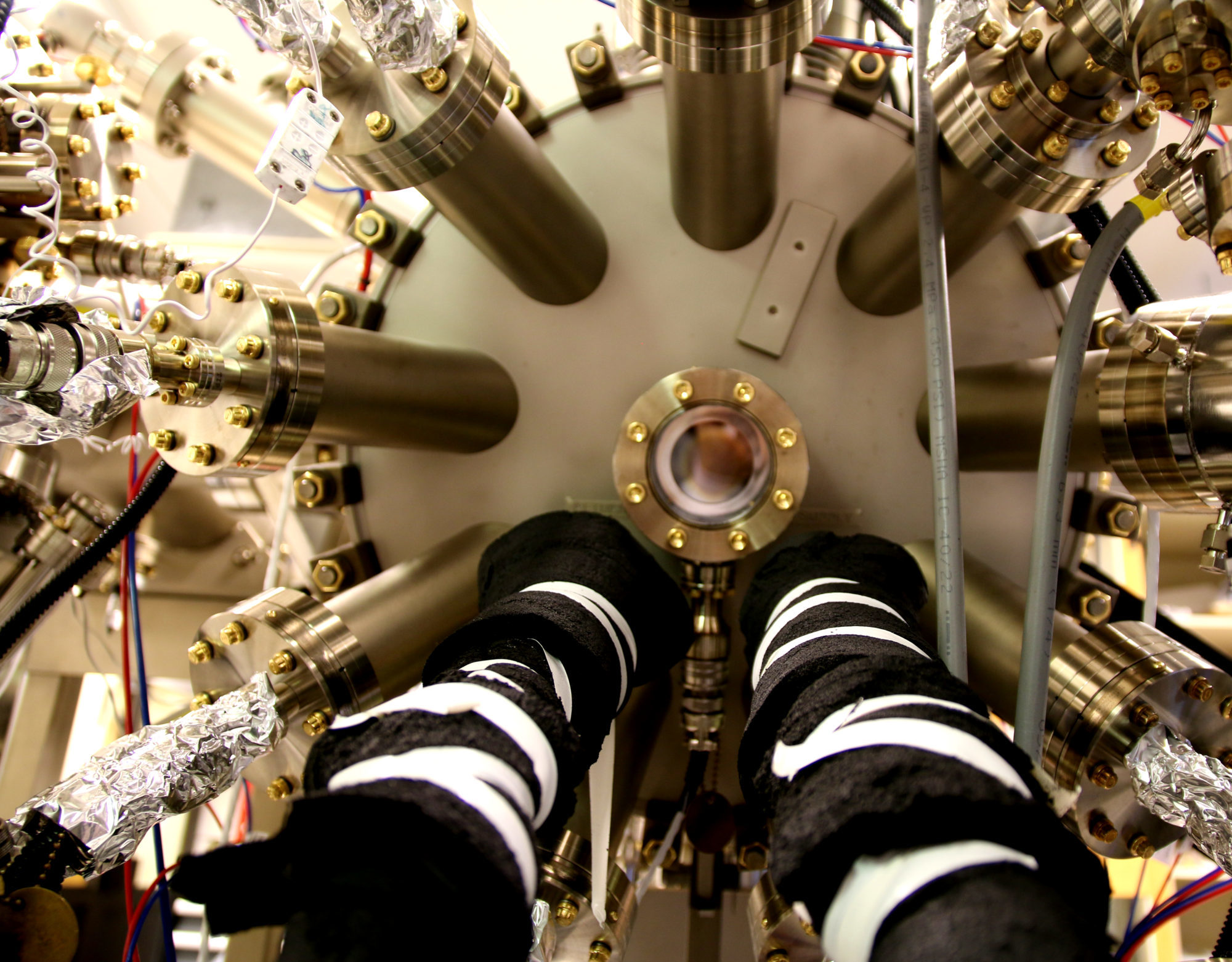
This molecular beam epitaxy machine enables researchers to alter microscopic structures. Photo: Idun Haugan / NTNU
Inside this new “MBE” machine, a research breakthrough has recently taken place. MBE stands for molecular beam epitaxy.
- You may also like: Nano-knowledge can lead to super solar cells
Special superlattice
Welcome to the world of nanotechnology, where quantum structures rule and constituents are so small that they’re measured in billionths of a metre: one nanometre (nm) is equal to 10e-9 meters (one billionth of a metre). The average human hair is approximately 100 000 nm thick. Nanometres are often used to measure the wavelength of light, and this breakthrough is about just that, specifically infrared light.
Wavelengths, light and radiation
- radio radiation (wavelength over 1 m)
- microwaves (1 mm - 1 000 mm)
- infrared radiation (700 nm - 1 mm)
- light (400 nm - 700 nm)
- UV light (wavelength 10 nm - 400 nm)
- X-ray radiation (0.01 nm - 10 nm)
- gamma radiation (anything below 0.01 nm)
Source: Wikipedia
The NTNU researchers who have been working with these miniscule units have managed to produce a nanowire with a very special superlattice. The result is a miniature laser in the form of a nanowire. It’s the uniformity of the superlattice that makes this miniature laser exceptional.
“The challenge is to get the superlattice structure consistent and even, so that the nanowire produces light at the same wavelength the whole way. Now we’ve managed to create this special superlattice inside the nanowires with the necessary regularity,” says Professor Helge Weman. He heads a research group that is working with the nanomaterials for this project.

The research team in front of the super machine: from left Bjørn-Ove Fimland, Dingding Ren, Lyubomir Ahtapodov and Helge Weman. Photo: Idun Haugan, NTNU
Weman’s colleagues Professor Bjørn-Ove Fimland, Ton van Helvoort, and the research team have made numerous nanowire-related research breakthroughs in recent years. In this latest breakthrough, PhD candidates Dingding Ren and Lyubomir Ahtapodov conducted the experiments that led to their promising results.
“They have a very good handle on this [process], and that control is the key,” said Weman.
The online journal Nano Letters published an article on their research findings earlier this year.
Structure of atoms inside the nanowires
A nanowire is several hundred times smaller than a human hair. Within each nanowire, the research group set up six superlattices consisting of ten quantum wells each. In order to obtain the uniform structure that forms the superlattice, the researchers created a very special structure using atoms.
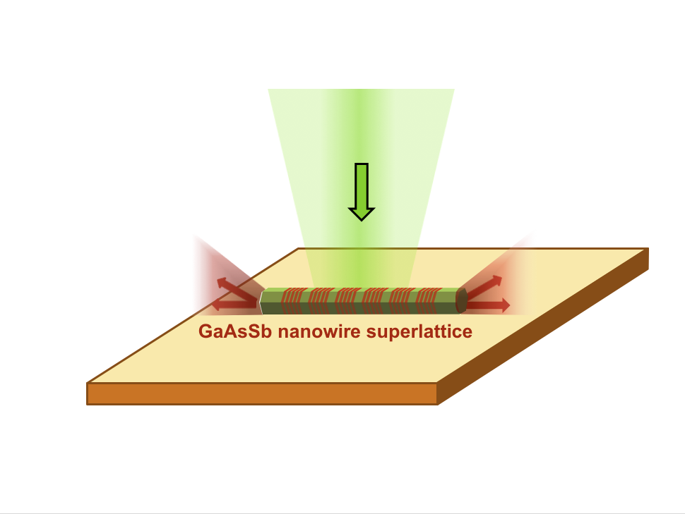
Schematic drawing of nanowires with six superlattices consisting of a total of 60 quantum wells. The laser emits infrared laser light (red arrows) from the ends of the nanowire when illuminated with a “pump laser” (green arrow).
The nanowires are built – or “grown” – by spraying the structure with different types of atoms. The atomic elements gallium and arsenic have created the basic structure, and the quantum wells contain antimony atoms as well. This atomic combination, plus semiconductors used to conduct power and create light, create the superlattice.
“The basic constituents are from two different groups in the Periodic Table: Group III and Group V. When we mix atoms from the two different groups we get what’s called three–five semiconductors. They’re well suited for generating light,” says Fimland.
- You may also like: Controlling problem ice — by cracking it
Creating light in a quantum well
By using a pump laser to transmit energy to the nanowires, electrons are released from the electron cloud surrounding the nuclei in the nanowires. The released electrons wander around – and many of them fall into the quantum wells. The electrons only have a short life span, and under certain circumstances the energy from them is transformed into infrared light.
Now we’re finally approaching the heart of this new miniature laser.
“Surplus electrons fall into quantum wells and create light. When the electrons fall from one level to another inside the wells, the energy is converted to infrared light,” explains Fimland.
Professor Bjørn-Ove Fimland and Postdoctoral Fellow Dingding Ren. Photo: Idun Haugan / NTNU
The infrared light consists of photons, which are the building blocks of all light. In this case, the photons clone each other so that they generate more and more identical photons.
The ends of the nanowire act like a mirror so that the light is reflected and sent back and forth through the nanowire. The uniform superlattice keeps the light’s wavelength steady, clear and sharp.
“Characteristic for a laser is that it shines at a very clearly defined wavelength. Our laser is in the infrared area at around 950 nanometres and has a very narrow wavelength,” said Weman.
Controlling the wavelength
When light is emitted at a particular wavelength, it is called lasing. If you get all the quantum wells to radiate light at the same wavelength, the whole lasing is reinforced. To achieve efficient lasing, the quantum wells must be as similar and uniform as possible so that the light is generated evenly up and down along the nanowire. Then the light builds in intensity throughout the length of the column.
Everything you wanted to know about nanotech
- Nanotechnology is one of the fastest growing research fields.
- It is a field of study that uses nanometres (nm) in working with atoms, molecules and units.
- Normally, nanotechnology is limited to structures smaller than 100 nm.
- By making small changes at the nano level, you can achieve big results at the macro level.
- The fields of physics, chemistry, biology, medicine and materials science have conducted nano-level research individually and used the term nanotechnology differently in the various fields.
- In recent years, everything nano-related has been gathered into one concept across academic fields.
- The research focus has shifted from basic research to applications.
“Six layers of superlattices containing ten quantum wells each make 60 quantum wells that all need to be as similar as possible. The challenge lies in achieving this state, and that’s what our researchers have now managed to do. No one has done this before,” said Weman.
Now that the researchers have gained this level of control in the process of growing nanowires and building superlattices, they can also direct and change the wavelength of the light. By injecting more antimony atoms into the well, the wavelength becomes longer and the energy level is reduced.
“You don’t always know what wavelength you’ll need for different applications. That’s why it’s so important to be able to precisely control and design the wavelengths by adjusting how much antimony is added to grow the nanowire,” Weman says.
- You may also like: After Big Oil comes the Age of Tiny Things
Not too thin, not too thick
When you work with such small structures, controlling the dimensions is a crucial factor. One of the challenges is to create the right size nanowires. If they’re too small, the light will leak out. And if they get too thick, the beam isn’t concentrated enough.
History of nanotech
- American physicist Richard Feynman envisioned the production of electronic circuits and machines on a molecular and atomic scale as early as 1959.
- The term nanotechnology was first defined by Japanese Professor Norio Taniguchi in 1974.
- President Clinton's National Nanotechnology Initiative was instrumental in putting nanotechnology onto the agenda in 2000.
- Since 2000, most industrialized countries have developed a strategy for the nanotechnology field.
“The thickness is extremely important when making lasers. Growing nanowires to the right thickness has been a goal since we started doing this research in 2006. Our nanowires were often too small and thin – but now, a good ten years later, we’ve managed to grow nanowires with the correct size,” says Weman.
- You may also like: New material may replace silicon
What can you use miniature lasers for?
“Looking ahead to the electronics of the future, the thinking is that information should be transmitted via optical laser pulses instead of via a transistor. For that you need to have really small laser sources, and our miniature laser is a step in that direction,” says Weman.
“The other thing we think will be interesting lies within medical applications. You need extremely small laser sources to be able to influence cells or molecules. For example, you could do spectroscopy with a resolution that is even better than can be done with a standard laser today.
The next goal for nano researchers is to establish and fund a larger project so that they can take the miniature laser research one step further.
“We can’t imagine where the technology will be needed yet. That’s how it was at the beginning when the first lasers came out. We didn’t see all the areas of application because they hadn’t been invented yet,” says Weman, adding that a lot of basic research remains to be done first.
The biggest remaining goal is to inject electrical current into the electrons in the laser. Then the researchers will have come a major step closer to being able to apply the technology.
Postdoctoral fellow Lyubomir Ahtapodov and Professor Helge Weman test the wavelength, or the emission spectrum, of the miniature lasers in the video below:
Reference:
Single-Mode Near-Infrared Lasing in a GaAsSb-Based Nanowire Superlattice at Room Temperature. Dingding Ren, Lyubomir Ahtapodov, Julie S. Nilsen, Jianfeng Yang, Anders Gustafsson, Junghwan Huh, Gavin J. Conibeer, Antonius T.J. van Helvoort, Bjørn-Ove Fimland, Helge Weman. Nano Lett. 2018, 18 (4), pp 2304-2310.