Great progress for electronic gadgets of the future
A new discovery is an important step towards smaller, more advanced electronics. And maybe more environmentally friendly gadgets, too.
Researchers at NTNU have found a completely new method to check the electronic properties of oxide materials. This opens the door to even tinier components and perhaps more sustainable electronics.
“We found a completely new way to control the conductivity of materials at nanoscale,” says Professor Dennis Meier at NTNU’s Department of Materials Science and Engineering.
One of the best aspects of the new method is that it does not interfere with other properties of the material, like previous methods did. This makes it possible to combine different functions in the same material, which is an important advance for nanoscale technology.
NTNU leading the work
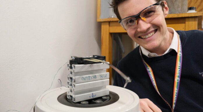
An enthusiastic Professor Meier says, “What’s really great is that this project is being run from NTNU and involves people from several departments. We also benefit from key facilities like the NanoLab and the TEM (transmission electron microscopy) Gemini Centre. This interdisciplinary approach shows what we can do when we work together.”
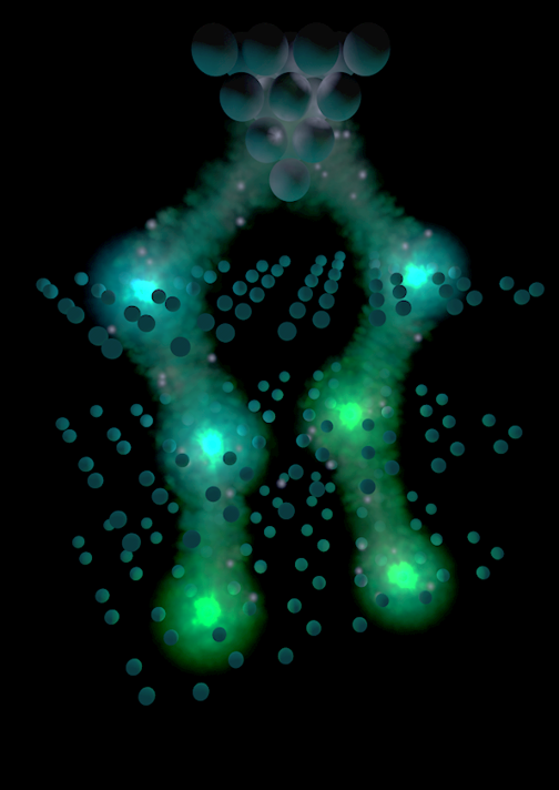
Using “hidden” defects at the atomic level can change the conductivity of the material while also maintaining its structural integrity. (Illustrated by Nanolayers Research Computing)
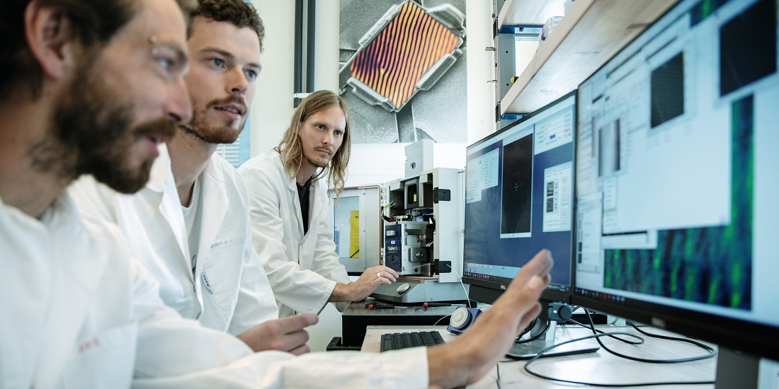
A new article in the prestigious and influential journal Nature Materials addresses the findings. The first authors are Donald M. Evans, Theodor S. Holstad, Aleksander B. Mosberg and Didrik R. Småbråten, who carried out innovative experiments and simulations in the Department of Materials Science and Engineering and the Department of Physics. The article has attracted international attention even before being printed.
The possibilities offered by the discovery were discussed in the August issue of Nature Materials by leading experts in the field.
Components mutually exclusive – until now
We rarely think about the technology that lies behind turning on a light bulb or our use of electrical appliances. The control of charged particles on a minute scale is simply part of everyday life.
But on a much smaller nanoscale, scientists are now routinely able to manipulate the flow of electrons. This opens up possibilities for even smaller components in computers and mobile phones that use barely any electricity.
A basic problem remains, however. You can simulate nanoscale electronic components, but some of the most promising concepts seem mutually exclusive. This means that you can’t combine multiple components to create a network.
“Utilizing quantum phenomena requires extreme precision to maintain the right ratio of different substances in the material while changing the chemical structure of the material, which is necessary if you want to create artificial synapses to simulate the properties of nerve pathways as we know them from biology,” Meier says.
Interdisciplinary collaboration
Collaborative interdepartmental efforts, led by Professor Meier, have succeeded in circumventing some of these problems by developing a new approach.
“The new approach is based on exploiting ‘hidden’ irregularities at the atomic level, so-called anti-Frenkel defects,” Meier says.
The researchers have managed to create such defects themselves, thus enabling an insulating material to become electrically conducting.
Defects in the material are related to its various properties. However, the anti-Frenkel defects can be manipulated in such a way that changes in the conductivity do not affect the actual structure of the material or change its other properties, such as magnetism and ferroelectricity.
“Maintaining the structural integrity makes it possible to design multifunctional devices using the same material. This is a big step towards new technology on a nanoscale,” says Meier.
The research team includes Professor S. M. Selbach from the Department of Materials Science and Engineering, Professors Antonius T. J. van Helvoort and Jaakko Akola and Associate Professors Per Erik Vullum and David Gao from the Department of Physics, and Associate Professor Jan Torgersen from the Department of Mechanical and Industrial Engineering.

Maybe the electronic gadgets of the future can be used longer. Illustration photo: Shutterstock, NTB scanpix
Erase and reuse
Another advantage of the new approach is that researchers can erase components on a nanoscale using a simple heat treatment. Then you can change or upgrade the components in the material afterwards.
“Maybe we’ll be able to use our electronic gadgets longer instead of recycling them or throwing them away. We can just upgrade them instead. This is fundamentally much more environmentally friendly,” Meier says.
Next step
Planning is already underway for further attempts to combine different components. This work will be carried out by the FACET group at NTNU’s Department of Materials Science and Engineering
That effort is supported by the European Research Council through an ERC Consolidator Grant that Meier received last year. The renowned Center for Quantum Spintronics (QuSpin) is also involved. The goal is to use both charge and spin in the electrons to give us a more environmentally friendly future.
Source: Evans, D.M., Holstad, T.S., Mosberg, A.B. et al. Conductivity control via minimally invasive anti-Frenkel defects in a functional oxide. Nat. Mater. (2020). https://doi.org/10.1038/s41563-020-0765-x