Engineering materials for a new generation of electronics
Harnessing a fundamental property of electrons called spin could help create a new generation of computer chips and faster, more stable and less power hungry devices. NTNU researchers are studying a type of material that could make this technology feasible.
Modern-day computers rely on the fact that electrons have charge. But electrons have another fundamental property called spin – a measure of magnetic orientation – that researchers hope to harness to create a new generation of computer chips. Spintronics – short for spin transport electronics – could lead to faster, more stable, and less power-hungry devices.
An electron’s spin is a bit like a compass needle that points north or south. Magnetic hard drives already use the spin of electrons to store information in the form of binary 0s and 1s, which your computer can then translate back into human-readable information. But traditional computer processing ignores spin entirely. Using spin for computation would mean processing and storage could happen on the same chip.
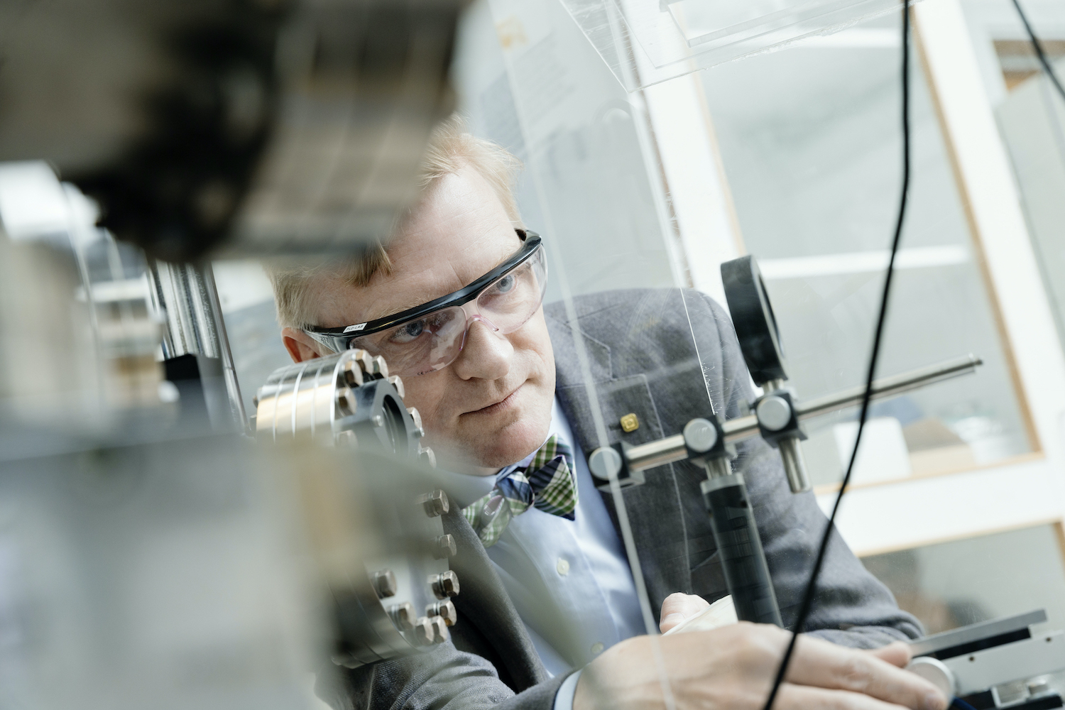
In most materials, there are equal numbers of electrons with spins that point in opposite directions, so from the outside they all appear to cancel out. These materials are known as antiferromagnetic, and Thomas Tybell, a professor in the Department of Electronic Systems at NTNU and his colleagues are looking for ways to engineer them for use in future spintronic devices. “If we use antiferromagnetic materials, where the spins cancel, they are very robust against perturbations,” he says.
- You might also like: When 80 microns is enough
Stability important
That stability is a big plus. Let’s say you’re working on an important document, and just before you hit save there’s a power cut. With conventional computing, you have probably just lost your work. But the spin of an electron stays the same even when the power is lost, so on a spintronic computer your work would be preserved.
But to create spintronic devices, we first need materials that allow us to reliably control spin.
One big challenge is engineering materials without internal boundaries that could mess with the spin of electrons and result in lost information. These boundaries – called domain walls – occur where the repeating pattern of atoms in the material doesn’t quite match up.
- You might also like: Great progress for electronic gadgets of the future.
Thin films are key
Recently, Tybell and his colleagues have found a way to make thin films from antiferromagnetic materials that look like they have no domain walls at all. By changing the arrangement of atoms – known as the lattice – in the substrate onto which the thin film is deposited, they can ensure the crystal grows in such a way as to avoid creating those internal boundaries. “Our key to controlling the physical properties is the lattice,” says Tybell.

The white and dark regions represent different magnetic regions, having their ‘compass needle’ pointing in different directions. The present study shows how to engineer materials with only one magnetic ordering. Data taken in collaboration with Ingrid Hallsteinsen, Rajesh Chopdekar (SLS), Erik Folven and Jostein Grepstad. Ref. I. Hallsteinsen, E.Folven, F. Olsen, R.V.Chopdekar, M.S. Rzchowski, C.B. Eom, J.K. Grepstad and T. Tybell, APL Matr. 3, 062501 (2015); licensed under a Creative Commons Attribution (CC BY) license.
“Previously we did see contrast between different magnetic regions as in the figure here. By controlling the lattice we suddenly got a grey, boring image with only one contrast, but actually what’s important is that each pixel has the same magnetic axis,” he says. “Suddenly you have no domain walls.”
In recent years other researchers have shown that it’s possible to create a single crystal that doesn’t have domain walls. This new work shows it is possible in thin films, too. “That’s important because suddenly you have unprecedented new possibilities for devices,” says Tybell. “If you want to make a device that works you can’t work on a single crystal, you have to make thin films.”
There are still a number of challenges to overcome before spintronics goes mainstream, and Tybell says he can’t be sure how long it will be until you’ll be able to hold an entirely spintronic computer in your hand. “It will depend on how well we can control the materials to allow them to be mass produced,” he says. “I hope it’s soon, but I fear it’s quite in the future.”
Transistors took time, too
The concept behind the transistors that are present in every computer around the world was first patented around 1925. It then took two decades until the first working transistor was realised by researchers working Bell Labs in the US, and several more years until they were in widespread use.
In the meantime, the materials Tybell and his colleagues are developing will not go to waste: they can also be used by researchers studying quantum objects from a fundamental physics point of view. And while it’s not easy to predict where that could lead, there’s always a chance it might prove vital in the future, one way or another.
“We should not forget that if you can grow single crystalline thin films, it opens up new avenues to study quantum phenomena and learn about these materials in a way that might be important for quantum technologies in the future,” he says. “I am sure there are many things still to discover.”