Solving a long-standing problem in transmission electron microscopy
Researchers at NTNU have come up with a remarkably simple method to solve a problem known as probe wandering in a transmission electron microscopy based technique.
For researchers wanting to understand the inner workings of magnetic materials, transmission electron microscopy is an indispensable tool. Because the wavelength of an electron is much shorter than the wavelength of visible light, a beam of electrons transmitted through a thin slice of a material can create an image in which the inner structure of the material is magnified up to 50 million times, many orders of magnitude more than with an optical microscope.
Since transmission electron microscopy, or TEM, was first developed in the 1930s, scientists and engineers have come up with many variations on the technique. Each of these variations suit different applications and come with their own advantages and disadvantages.
Now, researchers at NTNU have come up with a remarkably simple method to solve a long-standing problem in an almost 30-year-old TEM-based technique known as scanning precession electron diffraction, or SPED.
Fixing blurry images
First developed in 1994, SPED involves scanning a nanometre-sized electron beam over the specimen while rotating it a hundred times per second around an axis. The precessing motion of the beam while scanning helps to cancel out some interference-like effects that make it hard for researchers to resolve the structures they are studying. But researchers using SPED often run into a problem known as probe wandering.
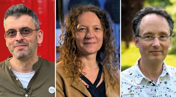
From left: Magnus Nord, Gregory Nordahl, and Emil Frang Christiansen. Photo: Anders Christian Mathisen.
In an ideal world, the lenses used inside a microscope would be free from defects, but in reality, defects are hard to avoid. These defects, known as aberrations, eventually cause the probe to wander away from the point a researcher is trying to image.
When the probe starts wandering, the result is a loss of resolution in the final image. “The resulting images become blurry,” says Gregory Nordahl, a PhD candidate in NTNU’s Department of Physics.
Lost spatial resolution
Nordahl first grappled with the problem of probe wandering when he tried to combine SPED with another TEM-based technique called STEM-DPC. In scanning transmission electron microscopy (STEM) rather than a broad beam surveying the whole sample at once, a focussed beam is scanned across the sample, line by line, to form an image.
Differential phase contrast (DPC) imaging is a technique that is sometimes used in conjunction with STEM – known together as STEM-DPC – to image magnetic fields in magnetic materials.
“When we first combined SPED with STEM-DPC, there was a lot of potential for improving the magnetic imaging capabilities,” he says. “Then we saw a huge downside, and that was the loss of spatial resolution.” Sometimes this loss of resolution is a trade-off that’s worth making, but in other cases, it can make the researchers’ investigations impossible.
Several images rather than just one
After Nordahl presented his results at a conference during the first year of his PhD, Lewys Jones, an assistant professor in physics at Trinity College Dublin in Ireland, got in touch with some ideas about how to fix the problem.
Together with Nordahl’s supervisor Magnus Nord, an associate professor in physics at NTNU, Jones came up with an ingenious solution to the probe wandering problem.
The method involves taking several images during one rotation of the electron beam instead of a single image, as is typical. “If we take a lot of images for each rotation of the beam, we can isolate the probe wandering,” says Nordahl. “Afterwards, it’s a simple programming puzzle to mix and match, overlap the images so that the movement is corrected for.”
The technique, which they have dubbed segmented SPED, or S-SPED, was detailed in a recent paper in the journal Ultramicroscopy. One benefit of the technique is that it doesn’t involve any extra equipment, or modifications to the existing microscope set up. “We are effectively increasing the resolution of SPED without any modifications to the TEM or its lenses,” says Nordahl.
New equipment made it possible
Nordahl says that the methodology the researchers developed could not have been possible without the use of direct electron detector technology. In a typical TEM set up, in order to create the final image, electrons are converted into photons as they pass through something known as a scintillator. But in a direct electron detector, the image is made from the electrons themselves. Norway’s first direct electron detector, MerlinEM, was installed at NTNU in 2020.
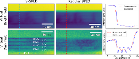
A comparison between S-SPED and regular SPED images. The resolution increase in S-SPED allows us to study the nanometre sized LSMO and LFO layers grown on a DSO substrate. Sample created by Yu Liu at the Department of Materials Science and Engineering. Graphic: Susanne Boucher, NTNU
The method was tested on a sample created from a CPU from an old computer. “My supervisor just essentially smashed it open with a hammer,” says Nordahl. Kasper Hunnestad, a PhD Candidate at NTNU’s Department of materials science and engineering then used NTNU Nanolab’s focussed ion beam to cut out a cross-section of the CPU for imaging.
Huge datasets — and a workaround
Putting the solution into action was not without its challenges. Multiplying the number of images taken means multiplying the amount of data the machine needs to collect by the same factor – for example, eight images per rotation means eight times more data – but the time it takes to complete one rotation doesn’t increase proportionally.
That means the machine is struggling to write all the data in the time available. “The datasets can be several hundred gigabytes large,” says Nordahl.
“You essentially record one of these images every one millisecond, and that is a lot of data going through at a very high speed,” he added. “A lot of the time the detector just couldn’t record it all, and you lost data.”
The workaround involved adding an extra rotation of the beam without recording any extra data, allowing the detector time to catch up.
Used to study tiny nano-sized magnets
Nordahl’s ultimate aim in combining STEM-DPC and SPED is to investigate what’s known as artificial spin ice systems. Artificial spin ices consist of tiny, nano-sized magnets arranged in a lattice-type structure that can be used to investigate magnetic phenomena. “Essentially, what you have are these islands that are magnetic, and areas in between that are not,” says Nordahl. “Due to stray fields coming from these magnets, they will interact with each other, and when you have enough of them, they will exhibit very interesting macroscopic properties.”
Now that the probe wandering problem has a solution, using the techniques to image magnetic materials containing elements just tens of nanometres in width will be possible.
The researchers are also already working on other applications of the new S-SPED technique that they hadn’t even anticipated before. “We have applied it to a lot of materials, and we are finding out more potential ways we can use it further,” says Nordahl. “The implementation is so simple, yet so effective, which is just mind blowing.”
Reference:
Gregory Nordahl, Lewys Jones, Emil Frang Christiansen, Kasper Aas Hunnestad, Magnus Nord. 2023. Correcting for probe wandering by precession path segmentation. Ultramicroscopy, Vol. 248
https://doi.org/10.1016/j.ultramic.2023.113715