Among the leaders in the hunt for the world’s tiniest electronics
Researchers in Norway are among those at the forefront in the field of nanoelectronics. Their goal is to create electronic components at the atomic level, which would open vast possibilities for electronic gadgets.
The latest issue of the internationally recognized magazine Nature Reviews Materials includes a review article on nanotechnology written by NTNU researchers. More specifically, it focuses on domain wall nanoelectronics, a field that might change a lot of what we know about electronic gadgets.
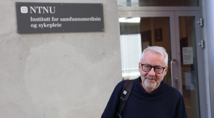
“Being invited to write this kind of article shows that the academic community has recognized the significance of our research,” say Sverre M. Selbach and Dennis Meier, both professors at NTNU’s Department of Materials Science and Engineering.

The researchers are investigating domain walls. If you don’t know what these are, there’s a fact box in the article to help. Illustration: amb design
It’s safe to say that the two professors leave it to others to do the boasting about their work. But only the very best researchers are invited to write review articles about their field in this magazine.
Not that Selbach and Meier are unfamiliar with getting attention. Since 2016, they have published more than 60 research articles on this emerging field, including in Nature, Nature Materials, Nature Nanotechnology and Physical Review Letters. They have also filed three patents and edited two books.
Atomic scale electronics
Selbach’s and Meier’s research groups rank among the very best in nanoelectronics, a field that has the potential to revolutionize our electronic gadgets. Researchers are trying to figure out how to replace today’s electronic components with even smaller and more energy efficient ones.
Our dream is to reduce the size of electronic components to the atomic scale and to use as little energy as possible.
In the Nature Reviews Materials article, Selbach and Meier provide an overview of how the field has evolved to where it is today, and also speculate on future possibilities.
Tiny gadgets that use almost no electricity are one potential development.
“Our dream is to reduce the size of electronic components to the atomic scale and to use as little energy as possible,” says Selbach.
“Ten years ago, nanoelectronics based on domain walls wasn’t really a research field. There were some bits of information here and there that a few groups scattered around the world were looking at. But it’s completely different now,” says Meier.
A whole community has now sprung up to investigate the possibilities of replacing traditional electronic components with domain-wall-based devices.
Article took two years to write
“We began writing this article two years ago,” says Meier.
“[Writing an article like this] is challenging, partly because they are often used in PhD courses and advanced master’s courses,” Selbach says.
So not only does everything have to be right, but the authors also have to provide a fair and balanced overview of previous and ongoing research, and of the many possibilities that lie in the future.
The professors conclude that we have very exciting times ahead of us – and they’ve only just begun to explore all the opportunities their research offers in developing atomic scale electronics.
Nanoelectronics in domain walls
For the past five years, the research groups led by Selbach and Meier have been working with nanoelectronics based on domain walls. So what is a domain wall, you ask? Well, that’s a little tricky to explain. But the fact box below should help.
What are domain walls?
- Some solid materials have built-in electric dipoles, which are pairs of positive and negative charges inside the material that are separated by a short distance. These materials are called ferroelectric.
- The electric dipoles can be rotated with an external electric field. Without the electric field, there are areas where all the dipoles point in one direction, and other areas where all the dipoles point in another direction. These areas are called domains and are separated by interfaces called domain walls.
- Ferroelectric crystals are electrically insulating. However, the domain walls can conduct electric current – much like a regular power cord, except that these walls are only a few atoms thick.
“We can send signals through the domain walls,” says Meier.
“We can send electronic signals through the domain walls and control their magnitude and shape,” says Meier.
The use of domain walls to mimic electronic components was proposed as early as the 1970s, Meier says. The concept remained in the realm of pure theory, partly because it wasn’t possible to measure the local properties of domain walls at that time.
“This has changed completely. Now the measurement methods are much better, and we can even model and predict the role that individual atoms play for the properties of a material,” says Selbach.
Imperfect materials do the trick
Today, the research team can manipulate single domain walls and use them to mimic electronic components like diodes, transistors and logic gates.

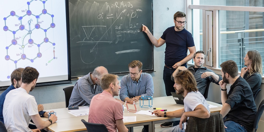
Dennis Meier in action in the laboratory. Photo: Geir Mogen, NTNU
The way they do this leverages the symmetry breaking that occurs within domain walls, and exploits the fact that crystal structures are never perfect.
“It’s old knowledge that the properties of a material are linked to their symmetry,” Meier says.” The German physicists Franz Ernst Neumann and Woldemar Voigt knew this already in the 19th century.
These properties also hold true at the atomic level. But domain walls are 200 000 times thinner than a human hair, so it isn’t easy to apply old knowledge at this small scale
EU has faith in the work
Different forms of advanced microscopy and simulations with supercomputers are absolutely key to successfully working with atomic level domain walls.
The research groups at NTNU benefit from key facilities like the NTNU NanoLab and the TEM Gemini Centre that have some of the most advanced nano-structuring and electron microscopy equipment in Norway, and from the national supercomputers operated by Sigma2.
The two professors may not brag about themselves unnecessarily, but they do like to boast about their colleagues at the centres and their many previous and current PhD students and postdoctoral fellows.
“We’re completely dependent on skilled and dedicated PhD students and postdocs who perform the very difficult and time-consuming measurements and simulations,” they say.
- You might also like: Great progress for electronic gadgets of the future
Coolest research lies ahead
Obtaining the financing for such an endeavour is a story in and of itself. All this sophisticated equipment and hiring talented people costs money.
“We never know if we’ll have money four years from now to keep pushing the limits,” says Meier.
Fortunately, the EU is also interested in the nanoelectronic possibilities. Two years ago, Meier received an ERC Consolidator Grant of more than 1.8 million euros. He also holds an Onsager Fellowship.
In addition to the EU, much of Selbach’s and Meier’s funding currently comes from the Research Council of Norway and various other support schemes. But raising money gobbles up a lot of time, even for this research team, which is among the best in the world. The two professors are very enthusiastic when it comes to their field and don’t spend too much time worrying about that.
“We have a lot of ideas that we want to test out,” says Selbach.
“The coolest research results are still ahead,” says Meier.
Reference: Dennis Meier and Sverre M. Selbach, Ferroelectric domain walls for nanotechnology. Nature Reviews Materials, doi.org/10.1038/s41578-021-00375-z (2021)