World’s tiniest circuit takes shape
Components are falling into place for the technology of the future. They can provide smaller, faster and cheaper electronics with minimal energy consumption.
Consumers are always eager to have the next new smaller, smarter electronic gadget.
But we are approaching a limit on how powerful our electronic components can be with the technology we’re using now. It is time to look for new solutions from a conceptual standpoint– like creating new kinds of networks for power transmission.
“Now we can emulate the behaviour of half-wave rectifiers – at the nano level,” says Dennis Meier, associate professor at NTNU’s Department of Materials Science and Engineering. A while ago, he and his colleagues successfully created a digital switch.
Electrical switches and rectifiers no longer trigger a sense of awe in us. They are parts in the technology that we use daily. For the most part, we’ve stopped being amazed by them.
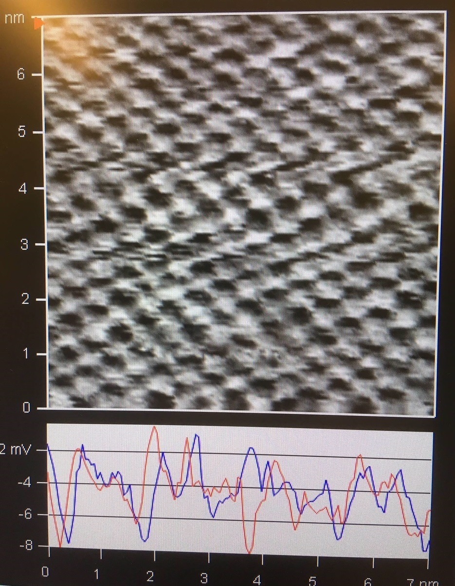
This is the kind of information that Meier and his colleagues get from the AFM. Photo: Dennis Meier/NTNU
But Meier is talking about something new: rectifiers that are one nanometre (nm) in size. One nanometre measures one billionth of a metre. In other words – extremely tiny.
Faster, smaller, colder
A rectifier is an electronic component that converts alternating current (AC) to direct current (DC). DC is electrical current that flows with steady power and in a constant direction. A rectifier enables the more variable AC power in socket outlets to be used for our electronic gadgets.
And although that is not exactly what we are talking about here, this new rectifier works in about the same way. The researchers have demonstrated a type of half-wave rectifier that blocks half of a signal’s wave using what is called a domain wall.
More about that later.
Their research is all part of something that one day may enable us to transmit stable signals even faster and on a much smaller scale, without heating things up, and with minimal use of electricity.
But not yet. Because this is still basic research.
- You may also like: On the topology of helimagnets and other difficult-to-understand things

Pretty soon you’ll be able to post selfies even faster than you can now. Photo: Colourbox
Can measure too
“What is really exciting is that we can recreate the functionality of key electronic components using domain walls, with walls that are 100 to 1000 times smaller than traditional components. This provides us with the potential for smaller, faster and cheaper electronics with minimal energy consumption,” says Sverre Magnus Selbach, who is also an associate professor in the same department.
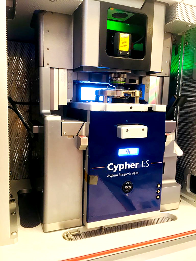
Not only did both researchers observe something at the nano level that resembles a rectifier, but they have also come up with a method to measure the activity in the rectifier. They did this using scanning probe microscopy (SPM) and dielectric spectroscopy at the nanoscale. (Do not fall off your seat now.)
Meier and Selbach are both part of a research group that has had their results published in the journal Nature Nanotechnology. https://doi.org/10.1038/s41565-018-0253-5
Less thermal development
So – what have they actually done?
You can apply electrical current to materials, transfer the signal into the material using a pure spin current and end up with electric current at the other end of the material. You can read more about that here, but the main point is that this method has several advantages, because the electrons are not involved in the transfer in the material itself.
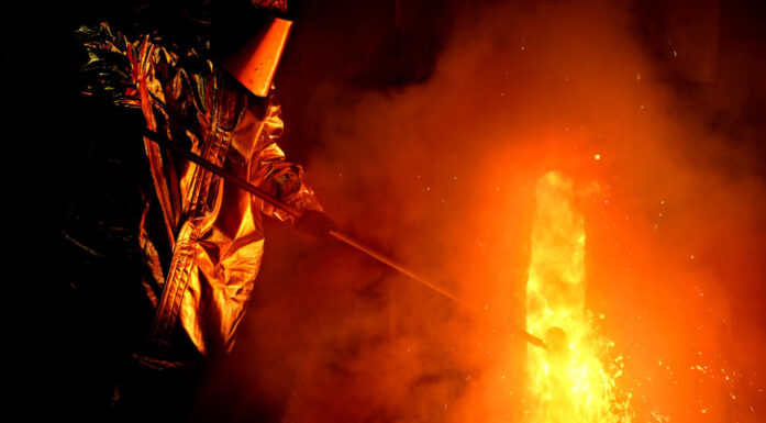
One advantage of an AC current is that it heats up less during transmission and yields faster control of the power. Heating is a significant limiting factor in today’s technology, and is perhaps the greatest impetus for wise heads to find new solutions so that we can have even faster gizmos.
The research team observed what happened when they applied alternating current to erbium manganese oxide (ErMnO3), a ferroelectric semiconductor.
Semiconductors have a crystal structure. If you enlarge them enough, you can see that the crystals are divided into distinct regions, each with their own special ferroelectric properties. These areas are called domains, which are separated by walls.
- You may also like: When 80 microns is enough
Signals in domain walls
These domain walls are the interesting part in this context: they can be used to transmit signals.
The research team examined signal transmission in the domain walls.
Electron microscopy and supercomputers enable researchers to use heavy calculations as a theoretical microscope. Photo: Donald Evans, NTNU
A rectifier is a necessary component to create a network that works at this scale. And this rectifier is what the researchers found when contacting the domain walls.
They applied a full wave at one end of the material and received half a wave at the other end – precisely the role of a half-rectifier.
Their work means that we now know more about the origins of rectifying properties. This has enabled the research group to combine state-of-the-art microscopy and atomic scale simulations on NTNU’s supercomputer Vilje.
“We are very fortunate at NTNU, with access to world-class electron microscopy and supercomputers. They enable us to use demanding calculations as a ‘theoretical microscope’ and run detailed tests of how we interpret the measurements,” says Selbach.
What now?
So what does this all mean? Have we come that much closer to new technology solutions, superfast computers and the devices we usually think of when we talk about the possible practical results of this type of research?
Even basic researcher Meier is apparently shifting his usual perspective a little. Maybe it is because he’s heard himself say that there are practical possibilities in his research so many times that he is starting to believe it himself, he surmises.
“We have single components that work. We can make a switch and a rectifier at this scale. We can’t yet connect these individual parts together. But we also have ideas on how to get there,” Meier says.
So, what this means is that they are on their way to creating a circuit at the nano level.
“This research is interesting because it enables us to design capacitors, inductors and transformers at the nano level. Applying alternating current instead of direct current is much more energy efficient and reduces waste heat,” says Meier.
Will they succeed? We don’t know. But we will probably know more soon.
Source:
Electrical half-wave rectification at ferroelectric domain walls. Jakob Schaab, Sandra H. Skjærvø, Stephan Krohns, Xiaoyu Dai, Megan E. Holtz, Andrés Cano, Martin Lilienblum, Zewu Yan, Edith Bourret, David A. Muller, Manfred Fiebig, Sverre M. Selbach og Dennis Meier. https://doi.org/10.1038/s41565-018-0253-5